
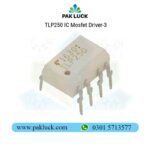


TLP250 IC Mosfet Driver
₨ 150 Original price was: ₨ 150.₨ 120Current price is: ₨ 120.
- Input threshold current: IF=5mA(max.)
- Supply current (ICC): 11mA(max.)
- Supply voltage (VCC): 10−35V
- Output current (IO): ±1.5A (max.)
- Switching time (tpLH/tpHL): 1.5μs(max.)
- Isolation voltage: 2500Vrms(min.)
| Weight | 0.15 kg |
|---|
TLP250 IC Mosfet Driver Price in Pakistan
The TLP250 IC Mosfet Driverare high voltage, high speed power MOSFET and IGBT drivers with independent high and low side referenced output channels. Proprietary HVIC and latch immune CMOS technologies enable ruggedized monolithic construction. Logic inputs are compatible with standard CMOS or LSTTL output, down to 3.3V logic. IR2110 output drivers feature a high pulse current buffer stage designed for minimum driver cross-conduction. Propagation delays are matched to simplify use in high frequency applications. The floating channel can be used to drive an N-channel power MOSFET or IGBT in the high side configuration which operates up to 500 or 600 volts.
Pin configuration isolated MOSFET driver TL250
The pin layout of TLP250 is given below. It is clearly shown in the figure that led at the input stage and photodetector diode at the output stage is used to provide isolation between input and output. Pin number 1 and 4 are not connected to any point. Hence they are not in use. Pin 2 is an anode point of input stage light-emitting diode and pin 3 is the cathode point of the input stage. Input is provided to pin 2 and 3. Pin 8 is for supply connection. Pin 5 is for the ground of power supply.

- Pin one and four is not connected to any point physically. Therefore they are not in use.
- Pin 8 is used to provide power supply to TLP250 and pin 5 is the ground pin which provides a return path to power supply ground. Maximum power supply voltage between 15-30 volt dc can be given to TLP250. But it also depends on the temperature of the environment in which you are using TLP250.
- Pin 2 and 3 are anode and cathode points of input stage LED. It works like a normal light-emitting diode. It has similar characteristics of forwarding voltage and inputs current. The maximum input current is in the range of 7-10mA and the forward voltage drop is about 0.8 volt. TLP250 provides output from low to high with a minimum threshold current of 1.2mA and above.
- Pin six and seven are internally connected to each other. Output can be taken from either pin number 6 and 7. Totem pole configuration of two transistors is used in TLP250. In case of high input, the output becomes high with output voltage equal to a supply voltage and in case of low input, the output becomes low with output voltage level equal to ground.
- Mosfet driver TLP250 can be used up to 25khz frequency due to slow propagation delay.
This all about pin configuration and working of TLP250. Now I will talk about how to used isolated MOSFET driver tlp250 as low side MOSFET driver and high side MOSFET driver.
Specifications:
- Input threshold current: IF=5mA(max.)
- Supply current (ICC): 11mA(max.)
- Supply voltage (VCC): 10−35V
- Output current (IO): ±1.5A (max.)
- Switching time (tpLH/tpHL): 1.5μs(max.)
- Isolation voltage: 2500Vrms(min.)
- UL recognized: UL1577, file No.E67349
- Option (D4) type
- VDE approved: DIN VDE0884/06.92, certificate No.76823
- Maximum operating insulation voltage: 630VPK
- Highest permissible over voltage: 4000VPK
- Creepage distance: 6.4mm(min.)
- Clearance: 6.4mm(min.)
TLP250 as a low side MOSFET driver:
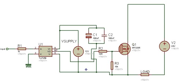
Circuit diagram of low side MOSFET driver using tlp250 is shown below. In this circuit diagram, tlp250 is used as a non-inverting low side MOSFET driver. you should connect an electrolytic capacitor of value 0.47uf between the power supply. It provides protection to tlp250 by providing stabilize voltage to IC.
As shown in figure above input is drive signal that drives the output. Vin is according to signal ground. It should not be connected with supply ground and output ground. It is clearly shown in above figure TLP250 and load ground is referenced to the power ground and it is isolated from input signal reference ground. When input is high, MOSFET Q1 get high signal from TLP250 and it is driven by power supply and current flows through the load. When input is low, MOSFET Q1 get low signal from TLP250 output pin and mosfet Q1 remains off and there is no current flow to load. Value of supply voltage ranges between 10-15 volt. Input resistor at gate of MOSFET is used depend on amplitude of input signal. Usually input signal is provided through microcontroller and microcontroller input signal level is in the order of 5 volt. Capacitor C1 is used as decoupling capacitor.
TLP250 as a high side MOSFET driver
Circuit diagram of MOSFT driver tlp250 used as high side driver is shown below. It is used as non inverting high side mosfet driver. Because input signal ground is connected to cathode of input stage light emitting diode. Therefore it is used as a non inverting high side mosfet driver.
In high side configuration there are three grounds as shown in figure above. Ground of input signal, ground of supply voltage and ground of power supply voltage. Remember that while using TLP250 as high side MOSFET driver, all grounds should be isolated from each other.
Buy MOSFET IGBT DRIVER TLP250 at Pakistan’s Best Online Shopping Store at cheap price. Here you get a wide range of Isolated Gate Driver IC. We Deliver in Gujranwala, Karachi, Lahore, Islamabad, Rawalpindi, Multan, Quetta, Faisalabad and all over Pakistan.
Package Include:
1x MOSFET IGBT DRIVER TLP250


MAECENAS IACULIS
Vestibulum curae torquent diam diam commodo parturient penatibus nunc dui adipiscing convallis bulum parturient suspendisse parturient a.Parturient in parturient scelerisque nibh lectus quam a natoque adipiscing a vestibulum hendrerit et pharetra fames nunc natoque dui.
ADIPISCING CONVALLIS BULUM
- Vestibulum penatibus nunc dui adipiscing convallis bulum parturient suspendisse.
- Abitur parturient praesent lectus quam a natoque adipiscing a vestibulum hendre.
- Diam parturient dictumst parturient scelerisque nibh lectus.
Scelerisque adipiscing bibendum sem vestibulum et in a a a purus lectus faucibus lobortis tincidunt purus lectus nisl class eros.Condimentum a et ullamcorper dictumst mus et tristique elementum nam inceptos hac parturient scelerisque vestibulum amet elit ut volutpat.





Reviews
There are no reviews yet.